Due to the intrinsic nature of the band gap of III-V semiconductors, they can be used in numerous optoelectronic devices (LEDs, laser, solar cells). Freiberger produces both N-type and P-type wafers in diameters from 3” to 8". Most segments of the optoelectronic market are very cost conscious, so we have worked with our customers to move to larger diameter wafers as a means to reduce cost.
Applications
Our processes start with high-purity raw materials such as gallium, arsenic, indium, phosphorus and ammonia, which are the main components of the semi-conducting and semi-insulating wafers manufactured at Freiberger. These wafers are supplied to epitaxial growth facilities where they undergo an epitaxial process to form layer stacks of ternary III-V compounds (Al/Ga/In/As/P/N). Then, using microelectronic technologies, RF-electronic devices (HBTs, HEMTs, BiFETs) or optoelectronic devices (LEDs, lasers, VCSELs, solar cells, photo detectors) are manufactured by device fabricators. Further downstream, equipment manufacturers (OEM) use these devices for their intended use in mobile phones, WIFI-systems, Radar applications, cars, traffic lights, TVs and PV systems.
Wireless Communication

III-V semiconductors have dominated wireless and high-speed applications such as power amplifiers and switches for cellular phones, smart and feature phones, WLAN enabled devices and the infrastructure supporting these capabilities.
These devices are also used for wireless broadband and Wi-Fi functionalities in PCs, notebooks and tablets, for cable TV, direct broadcast satellite, telecom, datacoms, social media, cloud and other modern technologies.
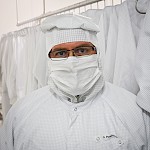
The mobile phones of the new generation offer more and more features; this means for us the quality of our products is most important. Our employees meet these quality requirements because competence and quality awareness are in perfect agreement.
Axel Porstmann, Shift Leader Final Cleaning
Optoelectronics