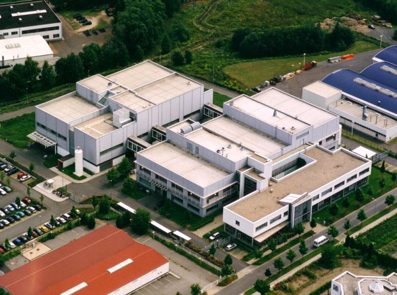
The new facility was constructed quickly, and production started there in 1997. In the same year Siemens (Infineon Technologies AG) acquired a minority share of 12.5 % in Freiberger. Sales increased rapidly, as the market welcomed a new player.
Over 50 years of experience Company History
A quick technological journey through time starting 1957
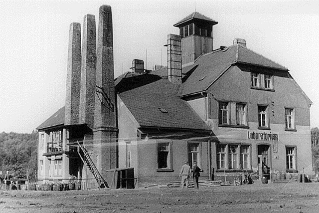
The roots of Freiberger can be traced to the formation of VEB Spurenmetalle Freiberg (SMF), a state-owned company established for the development and production of ultra-pure and semiconductor materials, such as Ge, Si, Ga, As, etc. SMF was spun out of the Institute of Non-Ferrous Metals, which was founded in 1949.
The Institute focused on developing technologies to produce the materials required by the electrical industry. Materials such as Zr, Ti, Ge, Si, P, and In were initially produced in pilot lines in the Institute’s labs. After the invention of the Ge transistor in the US, the electrical industry developed rapidly, and these pilot lines were no longer able to keep up with the demand, but eventually it became necessary to establish a separate company for the production.
So from 1957 on, VEB Spurenmetalle replaced the research Institute as the supplier of materials for East German industries. By the end of 1957, the company had 35 employees. Production took place in the labs of a former lead smelter.
 Administration building of Institute of Non-Ferrous Metals
 Pilot plant of the institute
1958
In 1958, the company is producing the first germanium.
1960

In 1960, a large-scale pilot production plant was built. It allowed the company to significantly increase its production of germanium dioxide, and to start growing germanium single crystals. At the same time, silicon became more and more important as an alternative to germanium. Not only was silicon much more readily available, but its electrical properties can be adjusted more easily by doping.
So in the mid-60s, a second pilot plant was set up for the production of semiconductor grade silicon. By the end of the decade wafer slicing technology was added to the production.
The 1970s and 1980s
During the 70s and 80s, the company continued to expand, with the production of silicon the main activity. Wafering technology was developed internally out of necessity. There were virtually no domestic supplier of the tools needed for this, and there was no hard currency available to purchase tools from the West.
In 1970, the company started its first R&D efforts to develop compound semiconductors, with the major emphasis on GaAs, GaP, InP, and InAs. Pilot line production of these materials began in 1982, and by 1987, GaAs, GaP, and InP were offered commercially. At the same time, demand for electronic grade silicon was growing rapidly. SMF expanded its silicon capacity to 120 tons/year by 1981, and added another plant in 1986.
") GaP/InP synthesis unit (self-development 1972)
GaP/InP synthesis unit (self-development 1972)
 HB GaAs single crystal puller in 1983 - 45 mm shoulder width
") LEC single crystal growth machine for GaAs in 1985 (2“)
LEC single crystal growth machine for GaAs in 1985 (2“)
 1988") LEC single crystal growth machines for GaAs and InP (2“) 1988
LEC single crystal growth machines for GaAs and InP (2“) 1988
1989
1989 was the time of political upheaval in East Germany. At that time, VEB Spurenmetalle had 1,800 employees, and manufactured over 450,000 silicon wafers, with a total area over 130 million square centimeters.
The road to a market economy is never easy. The Eastern markets that FEW had previously served no longer existed, and the quality of Freiberger’s Silicon wafers was not adequate for the Western free market. A new prospect arose in 1990, when Wacker decided to cease its GaAs activities. At this time, all experts agreed that GaAs was a material with great future potential. Wacker’s exit from the GaAs business would leave Germany without a domestic source for this strategic material. This provided a great opportunity for Freiberg, since SMF and FEW had been working for many years in the field of compound semiconductors. Although the technology and equipment were not state of-the-art, the knowledge, ability and commitment of a well-trained team was available. Financed by Treuhand and supported by local and federal funds, a contract with Wacker was signed to transfer the technology and equipment.
1990
")
With the breakdown of the state-controlled economic system, all state-owned companies were converted into capital companies and placed under the control of Treuhandanstalt, a federal agency created to prepare the companies for privatization. As of July 1 1990, VEB Spurenmetalle continued operations under the name Freiberger Elektronikwerkstoffe GmbH (FEW). Still today, the vendor code for Freiberger in wafer laser marks is FE.
1991
Equipment transport to Freiberg
However, during the following year, all efforts to privatize the company failed. FEW was still losing money, and no investors were attracted. As a result, the management agency downgraded FEW to a non-structurable firm. In such cases, the companies would be returned to Treuhandanstalt, and closed down. FEW was granted a final respite when Dr. Werner Freiesleben agreed to take over the management. Freiesleben’s concept was to not try to privatize the company as a whole, but to break it into segments, and privatize each separately. This plan worked, and, as a result, three companies were formed.
1992

After transporting the Wacker equipment to Freiberg, and transferring the technology, the first wafers using the process were produced during 1992. During this time FEW continued its efforts to adapt to the conditions necessary to compete in the free market. There were structural changes, spin-offs, reductions in workforce, etc. Eventually the company was deemed ready for restructuring, and handed over to a management agency to sell it.
1994
August 1, 1994: Bayer Solar AG (today SolarWorld AG), under the sponsorship of Bayer AG. It continued the solar silicon activities of FEW with 19 employees.
1995
On August 4 , the contract with Wacker is signed. Wacker Siltronic GmbH (now Siltronic AG) is founded with almost 300 employees.
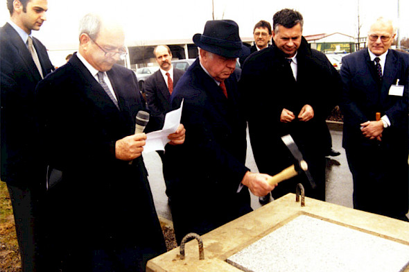
On August 31, Freiberger Compound Materials GmbH is founded with 81 employees. Just a few days later, the foundation stone is laid for the company's new headquarters.
1997
 1997")
1998
In 1998, Freiberger began mass production of 6" diameter LEC crystals and wafers.
1999
Sensing a shift in the market, Freiberger started to develop a 4” diameter VGF crystal growth process in 1999. Although Freiberger had only been in this facility for two years, the boom in wireless handsets, coupled with the increasing acceptance of FCM wafers, caused FCM to reach the capacity limits of the fab. Consequently, planning began for an major increase in capacity.
2000
In spring 2000, the cornerstone for Fab2 was laid. By this year, Freiberger had attained a 20% market share worldwide. Also in 2000, FCM demonstrated the first 6" diameter VGF crystal and the first 8" diameter LEC crystal.
2001
During 2001, even though the compound semiconductor market had crashed, Freiberger continued to expand its VGF capacity.
2002
Freiberger manufactured the first 8" diameter SI GaAs VGF wafer in 2002. New VGF technology and wire sawing technology were placed into production.
2010
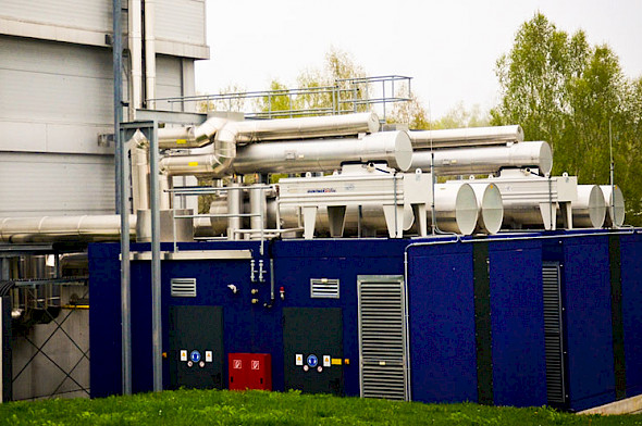
In an effort to both reduce costs, and to become a more “green” manufacturer, Freiberger placed a power cogeneration plant into operation. This plant currently produces about 50% of the power needed for the FCM fab. The overall efficiency of the plant is over 90%.
2013
Increases in both total market and market share tests the fab output limits.
A major expansion of the cleanroom provides significance capacity expansion to address market needs.
2015
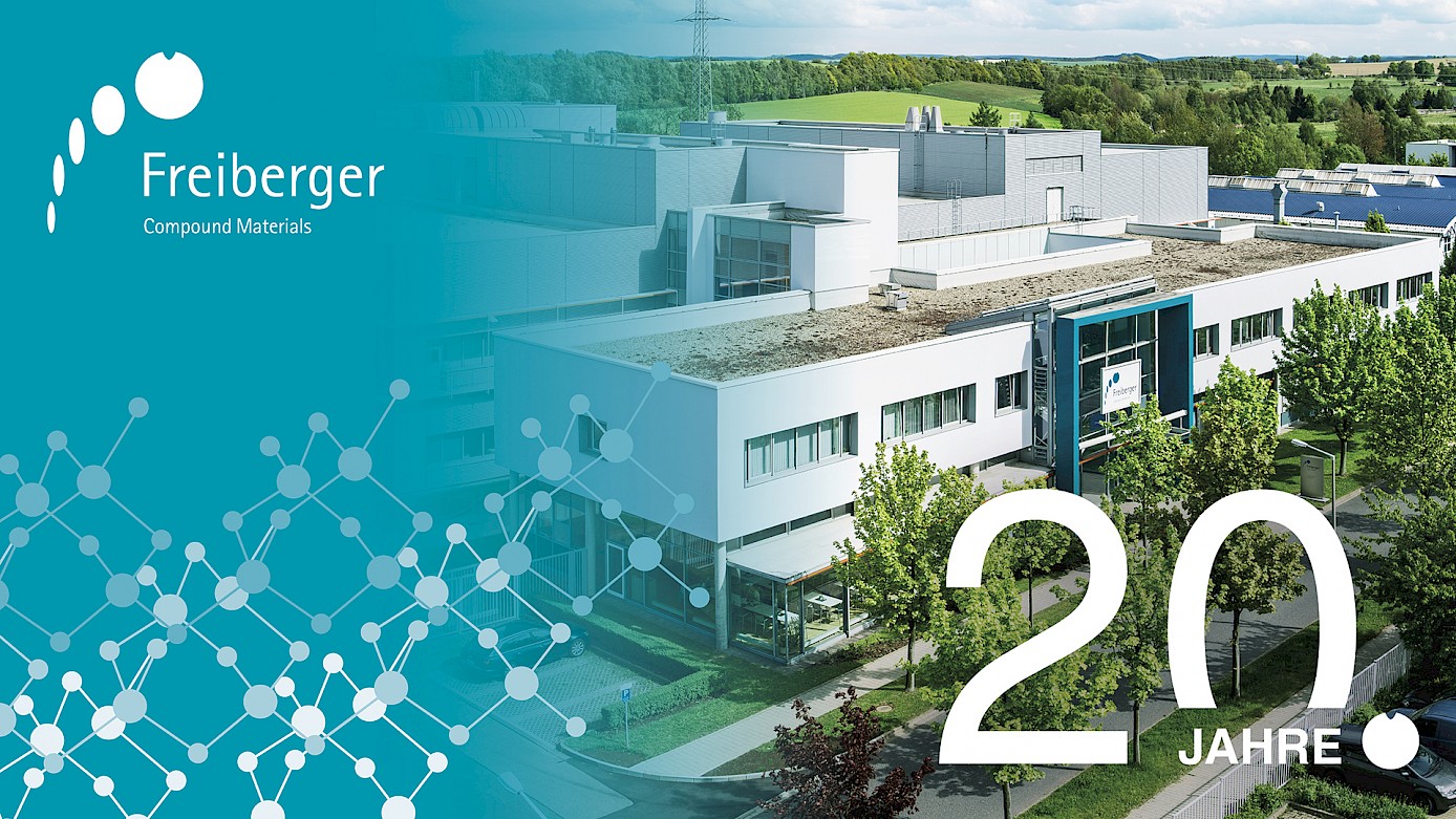
FCM celebrates its 20th anniversary