In a laser, this gain region is surrounded by an optical cavity, which channels the light in one direction. The cavity has partially reflecting mirrors on each end. As the light wave reflects back and forth, it continues to gain intensity due to stimulated emission. Once there is more amplification than loss (due to absorption and loss through the partially reflecting ends), the material starts to “laser.”
Optoelectronics
LEDs, laser, solar cells etc.

Both light emitters and light detectors rely on the formation of P-N junctions. Emitters work by applying an electric field, thereby generating photons (light output). Detectors work just the opposite – incoming photons generate electric fields. By tailoring the band gap of the semiconductor material involved, it is possible to adjust the wavelength of the light to be either emitted or detected. III-V semiconductor based devices are used as energy-saving solution in general illumination (LEDs), in the automotive industry, backlights in TVs and monitors and in the terrestrial photovoltaic market.
LASER
LASERs (Light Amplification by Stimulated Emission of Radiation) essentially work the same way as LEDs. Again, the applied electric field injects electrons and holes into the depletion region of the P-N junction, where they may recombine, creating a photon (spontaneous emission). But here, these photons may trigger other electron-hole pairs to recombine, creating additional photons, traveling in the same direction, and with the same phase as the original photon. This triggering of additional recombination is termed stimulated emission, and provides optical gain, which increases as the number of injected electrons and holes increases.
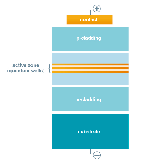
There are many different ways to create the optical cavity necessary for laser action, all of which create different types of lasers. One of the most common is known as a double hetero-junction laser. Here, a low band gap material (GaAs) is sandwiched between two higher band gap materials (AlGaAs). Both the injected carriers and the light emitted as a result of their recombination tend to be confined to the thin middle layer. [Drawing of DH laser] In this case, the wavelength of the emitted light will correspond to the band gap of this middle layer. By varying the material used in this layer, different wavelengths and be produced.
A more versatile way to confine the carriers in the active region is to create quantum wells epitaxially. As with the DH laser, both carriers and the emitted light are confined. Growing quantum wells with different energy levels produce lasers with different wavelengths.
All of the lasers discussed so far have horizontal optical cavities, so the light is emitted from one edge of the diode chip. It is also possible to produce lasers with vertical cavities. To do this, mirrors must be created during the epitaxy process. A superlattice using materials with different optical constants, and thicknesses equal to some multiple of the desired wavelength can produce a reflected light wave of opposite phase, getting either positive or negative rein-forcement as it passes each interface. Growing a totally reflecting mirror below the active region, and a partially reflecting mirror above the active region creates the vertical cavity. The light is then emitted vertically from the surface of the chip, instead of out the edge.
Most optical emitters are produced using MOCVD epitaxy today. In the past, and for some low-end LEDs even today, Liquid Phase Epitaxy (LPE) is used. In all cases the substrate is doped, in most cases N-type. In order to reduce costs, producers are gradually moving to larger diameters. LEDs are commercially made using everything from 2” to 6” diameter wafers. Most lasers are made using 3” or 4” diameter wafers.
VCSEL
VCSEL stands for "Vertical Cavity Surface Emitting Laser“, meaning the laser light is emitted vertically, or perpendicular to the wafer surface. The light is generated in an active AlGaAs structure similar to an “Edge Emitting Laser”. Planar Bragg reflectors function as mirrors, which are based on layers with alternating low and high refractive index (GaAs-AlAs).
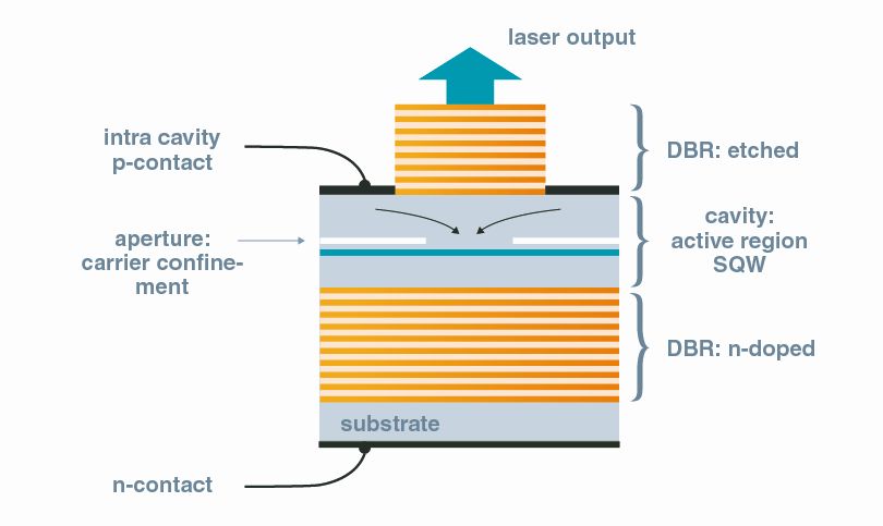
The complex layer stacks are generated with MOCVD. Depending on the power density within the active Laser structure, low-dislocation substrates have to be used.
Single VCSELs are used as optical transmitters for fiber optic data transmission and are suitable for analog broadband signal transmission. VCSEL arrays are used as light sources for 3D imaging and laser printers.
LED
The simplest semiconductor emitter is the LED (Light Emitting Diode).
The applied voltage drives electrons and holes to the P-N junction, where they recombine. Light, with energy of the band gap is emitted. This is termed spontaneous emission. For GaAs alone, this light is in the infrared. But with epitaxial layers of other materials, light can be generated with wavelengths ranging from the IR to the UV.
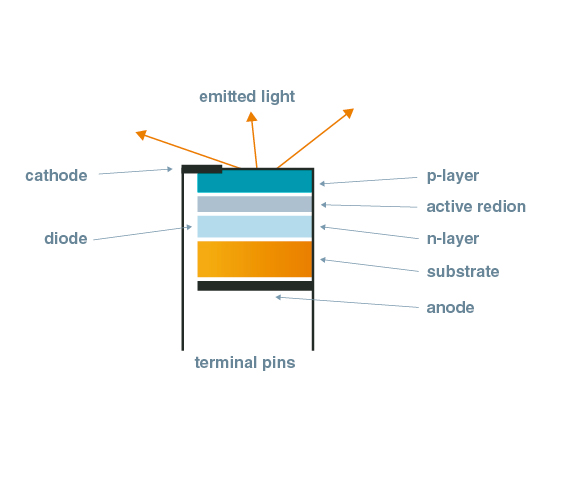
Since LEDs rely on the formation of a P-N junction, most are made by growing a P-type layer on an N-type substrate, although the opposite is also possible. To reduce costs, the epitaxy is grown using an MOCVD process, where the throughput is high.
Solar Cell
In emitters, an applied electric field injects carriers into the active region of a device, where they recombine, generating photons. For detectors, the opposite occurs. Incoming photons are absorbed by the material, generating electron-hole pairs, which are then swept away from the P-N junction by the electric field and collected.
Solar cells are a special class of detector, optimized to absorb as much as possible of the solar spectrum. While there are many different technologies used, the focus at Freiberger is on cells using GaAs as the substrate.
The efficiency of a cell is measured by what fraction of the input solar power is converted to electrical power. For GaAs-based cells, this can be as high as 33%.
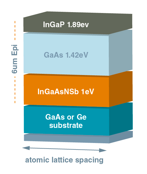
To improve the efficiency even further, it is possible to grow cells with multiple P-N junctions, with each junction grown in materials with different band gaps. Each junction absorbs a different portion of the solar radiation. By combining two, three, or even four junctions, it is possible to increase the efficiency to nearly 45%.
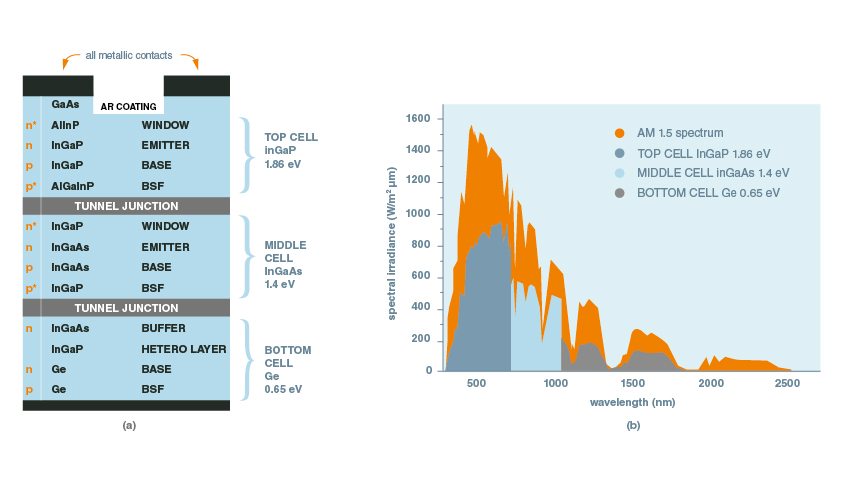
However, coupling the output from the different junctions make these cells significantly more complicated to produce. GaAs-based Solar cells (and other detectors) are produced using a variety of technologies currently, indicative of the immaturity of the industry. Typically MOCVD is used for the epi-taxy, although some multi-junction cells are grown using MBE. Likewise, either N-type or P-type wafers can be used as the substrate, with there being no current consensus. As the industry matures, most likely one technology will prove to be most economical, although this choice may be different for terrestrial systems than for space-based ones and for concentrator cells than for one-sun systems.