Wireless Communication

In this field of application, Freiberger’s 6" semi-insulating GaAs wafers are used for state of the art HBT, pHEMT and BiFET device production.

HBT

Hetero-junction Bi-polar Transistor

Hetero-junction bipolar transistors offer a performance improvement over standard bipolar junction transistors due to the use of different materials in the emitter, base, and collector regions of the device. Using a wider band gap material in the emitter allows the injection of electrons into the base region of the device.

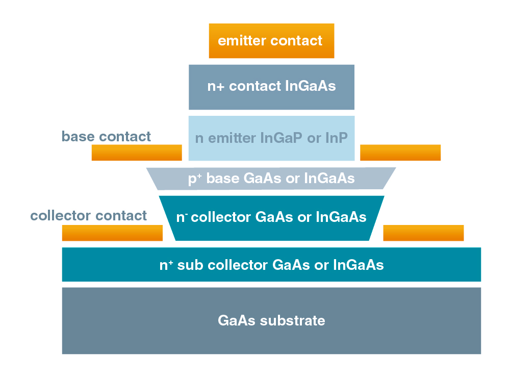
With proper choice of materials, the barrier for this electron injection is significantly lower than the barrier for backward injection of holes from the base into the emitter. Electron transport can be further improved by compositionally grading the base region. The band gap diagram below shows both the wide gap emitter and the graded base. The lightly shaded areas are the depleted regions in both junctions.

HBT structures can be grown using either MOCVD or MBE epitaxy, although the majority are currently made using MOCVD. For many years, the wide gap emitter material of choice was AlGaAs, but most recent HBTs use InGaP. The presence of Phosphorus also strongly pushes the epiaxy technology toward MOCVD. The structure is grown, starting with an N-type subcollector acting as a buffer layer.

The collector, also N-type is grown next, followed by the heavily P-type base layer, with the N-type emitter on top of the stack. Due to the relatively high current density, most HBTs are grown on low dislocation density VGF sub-strates. In an HBT, the electrons travel vertically through the device. As a consequence, the device size is quite small, allowing large numbers to be produced on each substrate. HBTs are primarily used in the production of power amplifiers necessary for wireless com-munication and data transfer.

pHEMT

(pseudomorphic High Electron Mobility Transistor)

A High Electron Mobility Transistor is a type of Field Effect Transistor, where band gap engineering has been used to dramatically improve the performance. By growing a heavily doped, wide band gap layer on top of a thin, undoped GaAs layer, a quantum well is formed. Electrons from the depletion region of the doped material fall into this well. Since this layer is undoped, there are no impurities to act as scattering centers for these electrons. As a result, their mobility is dramatically increased. If the temperature is reduced to near absolute zero, thereby freezing out the phonons, mobilities greater than 3 x 10⁶ cm² V⁻¹s⁻¹ have been measured. The electrons are confined to this thin quantum well, thereby forming what is known as a 2-dimentional electron gas.

Due to the thin layers and abrupt interfaces required in HEMT structures, nearly all early devices were grown using MBE epitaxy. Recently, however, MOCVD tools have improved to the point that currently either growth technology can be used. During the initial stages of epitaxy growth, the new layer grows with the same lattice constant as the substrate, thus forming a strained, pseudomorphic structure. As with the case of FETs, the electrons travel parallel to the wafer surface in pHEMTs. Consequently, the size of the device is significantly
larger than that of an HBT. On such a size scale, LEC wafers offer somewhat better electrical uniformity than VGF wafers. While LEC wafers are preferred, VGF wafers have also been used for pHEMT growth. pHEMTs are primarily used as high speed switches.

BiFET

As part of the continuing drive toward smaller, lower-cost circuitry in mobile phones, much effort has been focused on increasing the level of integration. By combining HBT functionality with FET switching capability in the same device, some of the bias control features can be embedded in the power amplifier. To do this, both HBT and FET structures must be fabricated from the same epitaxial stack.

Such a BiFET process is somewhat more complicated than growing or producing either device structure alone, but offers significant advantages in performance and overall cost structure. It is also possible to replace the standard FET with a HEMT, further improving the performance of the device. In this case, the pHEMT structure is grown first, and an HBT structure grown on top. The entire pHEMT forms part of the HBT sub-collector.