Technology GaAs / InP Wafer manufacturing

Freiberger produces the high quality GaAs or InP wafers using a series of processes, as shown in the chart below. These processes have been developed and improved through extensive testing and experimentation. In addition to our highly trained in-house technical staff, we have collaborative efforts currently underway with numerous research institutes throughout Germany, and with several of our customers.

Each process step is carefully monitored, with process control data automatically collected. The process flow can be best divided into four major areas: Synthesis, Crystal Growth (front end), Mechanical Wafering and Final Wafering (back end)

1 Synthesis

Raw Material 1.1

1.1 Raw Material

During synthesis, high-purity raw materials such as gallium and arsenic are chemically combined to form polycrystalline GaAs or indium and phosphorus to form polycrystalline InP. Due to the high vapor pressures of the Group V elements arsenic and phosphorus, the synthesis process is carried out at relatively high pressures and at corresponding melting temperatures of the compounds. The synthesized material is then melted and regrown using a highly controlled process to form single crystal ingots which can be processed into wafers.

High Pressure Synthesis of GaAs 1.2

1.2 High Pressure Synthesis of GaAs

The synthesis equipment consists of a high-pressure vessel, a graphite heater system including a heat insulation protecting the water-cooled walls. There are pressure-tight leadthroughs for electricity and inert gas supply and thermocouples. The pyrolytic boron nitride (pBN) crucible contains the gallium and arsenic (after the process the GaAs ingot). The charge is covered by liquid boron oxide encapsulates to avoid arsenic loss during the heat-up period. GaAs ingots up to 10inch can be obtained.

The synthesis process is started with vacuum pumping and purging with inert gas. During the heat- up period at temperatures between 400 and 600°C the boron oxide cylinder melts and covers the charge to avoid evaporation. At about 817°C arsenic melts and combines with gallium in an exothermic reaction. The inert gas pressure in the vessel must be higher than 35.8 bar (arsenic pressure at the triple point). The synthesized GaAs is heated up above the melting point (1238°C) and homogenized. The inert gas pressure rises to nearly 100 bar. Then the polycrystalline GaAs ingot cools down slowly. At the end of synthesis the crucible is taken out of the vessel and turned upside down in order to remove the ingot and to separate boron oxide from the synthesized material. After etching the material is ready for single crystal growth.

Clean working places and the well-organized sequence of processes are important elements of Freiberger’s clearly structured value chain, which supplies high-quality products for its customers

Andreas Szautner, Lead Man Mechanical Wafering

High Pressure Synthesis of InP 1.3

1.3 High Pressure Synthesis of InP

The InP synthesis is carried out in a quartz glass reactor at high pressure and at InP melting temperatures. Phosphorus is sublimated in a low-temperature zone at around 500°C and transported as a gas to a crucible with liquid indium. There the two elements react to form InP. After the chemical reaction is complete, the melt is directionally solidified so that non-stoichiometric components and impurities can be separated in the solid state. After subsequent etching, single crystals can be grown from the polycrystalline material.

2 Crystal Growth

Freiberger is unique in that we offer two different processes for growing the single crystal GaAs necessary for producing devices. Since the properties of the material grown by these two methods differ, this allows us to choose the process that will make wafers that best meet the technical needs of our customers.

Our Vertical Gradient Freeze (VGF) process makes material that is well-suited for devices with high current density (HBTs, LEDs, LASERs, etc.), whereas our Liquid Encapsulated Czochralski (LEC) method is best for larger area devices where the current density is not so high (Ion-implanted MESFETs, pHEMTs, etc.).

We only grow InP crystals using the VGF process in order to guarantee high structural perfection (i.e. low dislocation density).

VGF Crystal Growth Process 2.1

2.1 VGF Crystal Growth Process

In VGF equipment a pyrolytic boron nitride (pBN) crucible charged with pre-synthesized GaAs or InP and boron oxide is placed in a furnace assembled by a number of separately controlled zones which allow generating two nearly temperature-constant zones above and below the melting temperature and a controlled (small) temperature gradient in between.

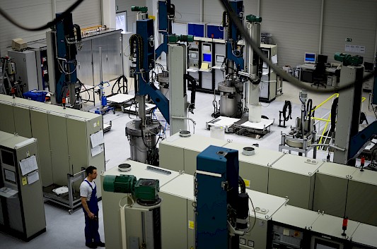
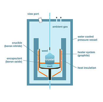
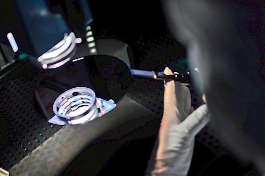
Crystal growth is initiated mostly by a <100>-oriented seed fixed in the lower part of the crucible and continued with an upward moving solid/liquid interface.

The temperature field is moved by a proper control of the heater system ensuring the given growth rate and interface shape. The low axial temperature gradient of typically below 5K/cm leads to crystals characterized by very low dislocation density.

LEC Crystal Growth Process 2.2

2.2 LEC Crystal Growth Process

The LEC equipment consists of a graphite heater system surrounded by heat insulation and a water cooled high-pressure vessel with pressure-tight leadthroughs for translation and rotation of crystal and crucible, respectively.

A crucible made from pyrolytic boron nitride (pBN) contains the GaAs melt covered by liquid boron oxide encapsulates to avoid arsenic losses during melt growth

By this technique, crystals up to a diameter of 150 mm (6inch) are grown. Multi-heater systems allow proper adjustment of the solid/liquid interface as well as temperature control of the crystal emerging from the boron oxide to avoid selective arsenic evaporation and to reduce residual strain. The pullers are equipped with a gas flow system to control C and O potentials and a fully computerized process and diameter control system.

The growth is usually carried out with counter-rotating seed and crucible at a growth rate of 5 to 10mm/h and <100>-seed orientation in a nitrogen- and CO-containing atmosphere at a pressure of more than 0.2MPa.

Annealing of GaAs LEC Crystals 2.3

2.3 Annealing of GaAs LEC Crystals

The GaAs LEC crystals have to be are annealed for stress relaxation, adjustment of EL2- concentration and improvement of macroscopic and mesoscopic electrical and optical uniformity. Annealing influences size distribution and arrangement of Arsenic precipitates as well.

Crystal Analysis 2.4

2.4 Crystal Analysis

After the crystal has been grown, it must be characterized. Freiberger has one of the most thorough analysis and metrology labs in the industry. This allows us to prove the quality of our material.

Samples from the seed and tail ends of each crystal are sliced and prepared for various types of analysis.

The first parameter to be measured is the crystalline perfection of the crystal. This is done by dipping the sample into molten potassium hydroxide (KOH) for GaAs or a etchant containing hydrobromic acid (HBr) for InP. Wherever a dislocation intersects the sample surface, the KOH/HBr etches a small pit. The density of these etch pits (EPD) is a measure of the lattice perfection of the crystal. Using a scanning system, we then measure every etch pit on the sample wafer. [EPD scan] The electrical parameters of seed and tail samples are also measured for every crystal. While this is done using standard Hall/van der Pauw measurements, we can also map the resistivity across the wafer contactlessly, using a COREMA tool. [COREMA map] Contactless electron mobility maps may also be obtained with this tool.

Several parameters combine to determine the electrical properties of the crystals. For GaAs, the two most important are the concentrations of carbon and EL2 (an electrically active defect related to an As-on-Ga antisite in the lattice). We can measure both of these concentrations. Carbon is measured using FTIR localized vibrational mode spectroscopy, and EL2 is measured with IR absorption spectroscopy. The concentration of the dopants of the InP (sulphur or iron) is determined by chemical analysis. [EL2 map] IR spectroscopy, as well as Photoluminescence topography can also be used to measure the distribution of dopants or carrier concentration. [PL map]

From raw material to saleable wafer, Freiberger’s production speed is high as compared to its competitors. The underlying principles of our technology are efficiency, stability and quality based on a close interaction of R&D and production.

Michael Rosch, Group Manager Technology Crystal Growth

3 Mechanical Wafering

Converting a GaAs/InP crystal into wafers requires a number of steps. The initial processes take place in what looks like a high-tech version of a machine shop. Semiconductor wafers have extremely exacting geometrical tolerances, so every step must be carefully programmed, and automated as much as possible.

Crystal Grinding 3.1

3.1 Crystal Grinding

The crystal is fixed at its front sides in the cylinder grinding machine. For this purpose, special bars are mounted on the front sides. This allows fixing the crystal between centers in the cylindrical grinding machine. As tool a diamond pot- grinding- wheel is used.

After determination of <110> directions the crystal is positioned in the grinding machine according to desired flat/ notch direction and the flat/ notch is ground in the required orientation with regard to the <110> directions.

Crystal Sawing 3.2

3.2 Crystal Sawing

Inner Diameter Saw (ID Saw)

The cylindrically ground crystals are mounted on a beam. After orientation into <100>- direction to the front side the ingot is positioned at the ID saw (inner diameter saw) according to the desired orientation. With a diamond ID saw blade wafers are cut from the ingot.

Wire Sawing

The wire sawing is an alternative cutting method to ID sawing. Cutting is carried out by moving a slurry-carrying wire through the crystal. Compared to ID sawing, the crystal is cut by one move which increases sawing efficiency.

Edge Rounding

After sawing the wafer will be edge ground. The edge is ground to remove the damage of prior grinding steps. This also provides an optimal edge profile for the customer. By edge grinding the final diameter is adjusted. The position of the flat/ notch is measured and ground in the required orientation.

Etching and Cleaning 3.3

3.3 Etching and Cleaning

After sawing, edge grinding and surface grinding the wafer is etched. There are two steps of etching. The first step comprises ultrasonic cleaning and short- time- etching. The cleaning station is designed to remove particles and organic or inorganic films from the wafer surface.

The second step is damage etching. Wafer thickness is reduced by 12µm. In this wet chemical step damage layers resulting from sawing, edge grinding, surface grinding and laser marking are removed.

Feiberger encourages its employees to play an active part in the company and participate in job training. We are a good team and give first priority to quality.

Steffi Grond, Lead Man, Metrology

4 Polishing and Cleaning

For most of today’s III-V-semiconductor based devices, the surface of the substrate is the most critical feature of the wafer. The flatness of the surface, the number and type of impurities on the surface, and even thickness and composition of the oxide can all play crucial roles in how well the device performs. It is extremely important how this surface is prepared, and how well the surface can be duplicated on every wafer from every boule.

Polishing 4.1

4.1 Polishing

Polishing of GaAs wafers is a chemical/mechanical process (CMP). The surface is oxidized by means of a chemical reagent in the polishing fluid. The reaction product is removed using the mechanical component of the polishing fluid and the polishing pad.

FCM wafers are polished in two steps – “Pre-polishing” (stock removal) and “Final polishing”. These two steps are different with respect to obtainable surface quality and applied polishing media (pads, fluids, pressure). Therefore, different polishing tools are used.

Double Side Polishing

After etching and thickness measurement the wafers are pre-polished (stock removal step) to remove surface and subsurface damage resulting from previous working steps and to generate the required geometrical properties of the wafer. The figure shows the double side polishing technology. Between upper and lower rotation polishing plates covered with polishing pads the wafers rotate in carriers driven by ring and sun gear.

The polishing fluid consists of chemical reactor and mechanical slurry and is fed to the rotating polishing plate through holes in the upper plate. Wafers of bigger diameters meeting the highest flatness requirements are double side polished.

Single Side Polishing

The alternative to double side polishing is the single side polishing technology as shown in the figure. It s used as pre-polishing (stock removal) step for customers, who prefer as cut/etched wafer back sides, and generally in final polishing. For polishing the front side, the wafers are mounted on ceramic polishing blocks.

The blocks rotate upside down on the rotating, pad-covered polishing plate. To obtain a good polishing result, a defined quantity of polishing fluid, surface pressure and velocity kinematics play an important role.

Cleaning 4.2

4.2 Cleaning

After the wafers have been polished, they go through a cleaning process. This step not only removes any particles but also “resets” the oxide present on the wafer surface. Since the wafer surface is so critical, each wafer undergoes a thorough inspection.

Quality Control 4.3

4.3 Quality Control

The surface of every wafer that leaves the cleaning line is carefully examined for visible defects by high-resolution microscopes and highly qualified employees under a bright light source.

After passing this initial scrutiny, cassettes of wafers are scanned for particles using a Surfscan, and then measured for flatness with an Ultrasort.

Numerous other surface properties can also be measured. The concentration of any residual surface impurities can be measured using total reflectance x-ray fluorescence (TXRF). We look at the condition of the oxide layer using ellipsometry. And the microscopic roughness of the surface can be measured using either white light interferometry or atomic force microscopy. Undergoing this battery of tests ensures that every wafer meets the specification under which it was produced.

Packaging and Certification 4.4

4.4 Packaging and Certification

The final steps in the process is to package the wafers in cassettes, and sealed in both polyethylene and foil bags. The cassettes are then properly labeled and all the necessary documentation is prepared.

By maintaining complete traceability throughout the manufacturing cycle, Freiberger can provide complete information for every wafer that is shipped.

You meet all types of people at Freiberger; I enjoy working with them, solving problems together and thus contributing to the further advancement of the company.

Romy Krautwald, Lead Man Final Cleaning