GaAs Wafer

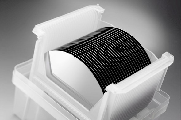
We manufacture semi-insulating and semiconducting gallium arsenide substrates with diameters from 3" to 8" for high-frequency and optoelectronic applications.

Freiberger has established a worldwide reputation as supplier of products that meet highest quality standards.

In our elaborate analysis and measuring processes all products undergo a comprehensive characterization enabling us to meet the customer requirements.

Our wafers are manufactured from LEC or VGF grown GaAs single crystals GaAs. The required electrical properties are obtained by adding dopants such as carbon, silicon, tellurium or zinc. The result is n-type or p-type high-resistance (>107 Ωcm) or low-resistance (<10 - 2 Ωcm) semiconductors. The wafer surfaces are generally epi-ready (extremely low contamination) i.e. their quality is suitable for direct use in epitaxy processes.

Physical Properties

Crystal structure Zinc blende
Lattice constant (300K) 5.654 Å
Atomic density (300K) 4.43 ×1022 cm-3
Melting point 1238 °C
Density (300K) 5.315 g cm³
Linear thermal expansion coeffi cient (300K) 6.03 ×10⁻⁶ K-1
Thermal lattice conductivity (300K) 0.48 W cm-1 K-1
Specific heat (300K) 0.325 J g-1 K-1
Energy gap (300K) 1.42 eV
Electron mobility (300K) 8800 cm2 V-1 s-1
Hole mobility (300K) 450 cm2 V-1 s-1
Effective electron mass 0.068 m0
Intrinsic electron concentration 1.8 ×106 cm-3
Intrinsic resistivity (300K) 3.8 ×10⁸ Ωcm
Static electric constant (300K) 12.85
Optic electric constant (300K) 10.88
Elastic constants
C11
C44
C12

11.88 * 1010Pa
5.49 * 1010Pa
5.38 * 1010Pa
Mohs hardness 4.5
Vickers hardness for (0.05 .. 1) N 6.52 * 109Pa
Surface energy
{ 100 }
{ 110 }
{ 111 }

220 ×10-6 J cm-2
150 ×10-6 J cm-2
130 ×10-6 J cm-2

Standard Definitions

Wafer flatness is determined by means of an interferometry measuring equipment using a focal plane on front surface as a reference plane (edge exclusion is 3 mm).

TTV (Total Thickness Variation)

... the difference between the maximum and minimum thickness values of a slice or wafer. Wafer clamped.

TIR (Total Indicated Reading)

... the distance between the maximum and minimum distances of the median surface from a reference plane. Wafer clamped.

Bow

... a measure of concave or convex deformation of the median surface of a slice or wafer, independent of any thickness variation which may be present. Wafer unclamped.

Warp

... the difference between the maximum and minimum distances of the median surface of the slice or wafer from a reference plane. Wafer unclamped.

General Definitions

Lot - for the purpose of definitions,
a) all the wafers of nominally identical size and characteristics contained in a single shipment, or
b) subdivisions of large shipments consisting of wafers as above which have been identified by the supplier as constituting a lot, or
c) often refers to all wafers cut from a single boule.

Dopant - a chemical element, usually from the second, fourth, or sixth columns of the periodic table for the case of III-V compounds, incorporated in trace amounts in a semiconductor crystal to establish its conductivity type and resistivity.

Orthogonal Misorientation - in {100} wafers cut with intentionally "off-orientation”, the angle between the projection of the vector normal to the slice surface onto the {100} plane and the projection on that plane of the nearest direction. It refers to the error in the direction, not the magnitude of the off cut angle. SEMI-Standard value is ±5 degrees.

Mandatory criteria Optional criteria
Nominal diameter Crystal growth method
Thickness (see applicable standards for various diameters) Etch pit density
Total Thickness Variation (TTV) Dopant type
Surface Orientation Electrical resistivity
Lot acceptance procedures Electron mobility
Certification Carrier concentration
Packaging and Labeling Surface condition